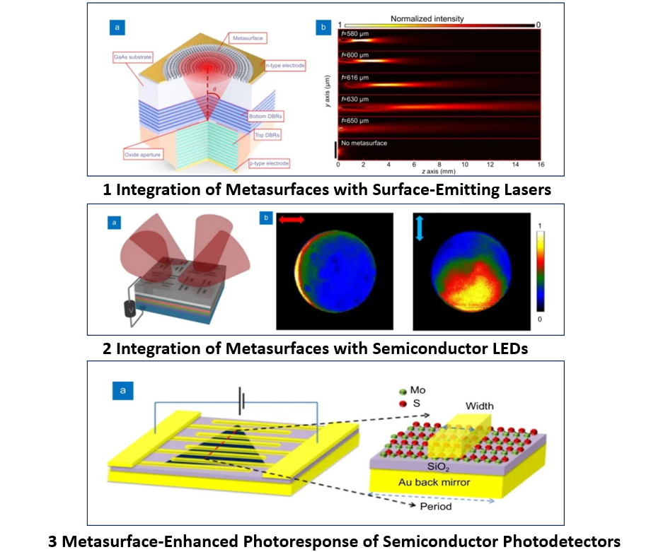
Since the invention of the first semiconductor laser in the early 1960s, semiconductor optoelectronic devices have achieved remarkable commercial success and have profoundly influenced modern life in areas ranging from communication, lighting, and entertainment to medicine. In recent years, the rapid emergence of new application fields, such as consumer electronics, AR/VR displays, and sensing, has placed increasing demands on the performance enhancement and functional expansion of semiconductor optoelectronic devices. Against this background, the miniaturization and integration of optoelectronic devices and systems, as well as the realization of multifunctional operation and multitasking, rely on innovative on-chip integration solutions.
Artificially structured interfaces composed of nanoantennas, known as optical metasurfaces, are regarded as a disruptive nanophotonic technology. By controlling the geometry and artificial arrangement of meta-atoms, metasurface elements can precisely manipulate the amplitude, phase, polarization, and other physical properties of electromagnetic waves. They are expected to replace bulky refractive optical components and promote the miniaturization and integration of optical elements. At present, optical metasurfaces can be generally divided into two categories according to their material properties: plasmonic metasurfaces and dielectric metasurfaces.
Over the past decade, optical metasurface technology has been widely applied to various functions, including imaging, holography, beam shaping, advanced displays, and optical measurements. Optical metasurfaces also provide an important research platform for exploring new optical functionalities, such as generalized Pancharatnam–Berry phase and topological phase, helping to reveal new mechanisms for wavefront manipulation using micro/nano-optical structures. On the other hand, the planar configuration of optical metasurfaces and their compatibility with CMOS fabrication technology make them highly suitable for on-chip integration with semiconductor optoelectronic devices. The vertical integration of optical metasurfaces onto semiconductor optoelectronic devices provides a feasible route toward miniaturized, integrated, and multifunctional optoelectronic systems.
Prof. Pei-Nan Ni from the School of Physics, Zhengzhou University, Prof. Yi-Yang Xie from Beijing University of Technology, and Prof. Patrice Genevet from the Colorado School of Mines published a review article entitled “On-chip light control of semiconductor optoelectronic devices using integrated metasurfaces” in Opto-Electronic Advances. This review summarizes recent advances in using integrated optical metasurfaces to control and enhance the properties of semiconductor optoelectronic devices. The article focuses on representative device platforms, including semiconductor lasers, semiconductor light-emitting devices, semiconductor photodetectors, and low-dimensional semiconductor devices. It discusses the applications and advantages of optical metasurfaces in optoelectronic integration, including improving the beam quality, polarization control, and wavefront shaping of edge-emitting and surface-emitting lasers; tailoring the emission properties of semiconductor light-emitting devices; enhancing the photoresponse, polarization and wavelength detection, and vortex-beam detection capabilities of semiconductor photodetectors; and strengthening light–matter interactions in low-dimensional materials. The article also analyzes and discusses future development trends of integrated optical metasurfaces.
This work was supported by the National Natural Science Foundation of China, the Natural Science Foundation of Henan Province, the China Postdoctoral Science Foundation, and the Beijing.